


PCB jari emas anti-pengoksidaan
Hoshineo LCD-Tech memainkan peranan penting dalam elektronik, semikonduktor, industri litar bersepadu, dengan menjual pelbagai pCB jari anti-pengoksidaan emas, untuk memberi sokongan untuk rantaian industri PCB hulu dan perusahaan hiliran. Dengan kelebihan kedudukan industri, pengangkutan yang mudah dan operasi fleksibel, Syarikat mempunyai daya saing tertentu di pasaran, dan produknya dieksport ke Eropah, Amerika dan Asia Tenggara.
Hantar Pertanyaan
Penerangan Produk
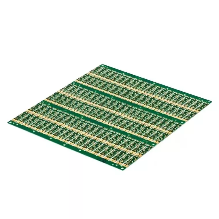
The Anti-Oxidation Gold Finger PCB produced by Hoshineo Lcd-Tech is a special form of PCB (Printed Circuit Board, printed circuit board), which combines Goldfinger technology and antioxidant treatment process. Gold finger is a special connection structure on the PCB board, which designs one end of the PCB board into a shape that can be inserted into the connector card slot, and contacts the solder pad or copper sheet on the PCB board through the connector pin, so as to realize the external connection and signal transmission of the circuit board. Because this structure presents a finger shape on the PCB board and is usually plated with antioxidant materials such as gold or nickel gold, it is called Anti-Oxidation Gold Finger PCB.
Hoshineo Lcd-Tech China Anti-Oxidation Gold Finger PCB product parameters:
| ITEMS | Parameter | |||||
| Number of Layers | 1-20 layers | |||||
| Board Materials | FR4,CME3,CME1,5G | |||||
| PCB Size (Min- Max) | 50x80mm to 1000mm×600mm ( 39.37"x23.6") | |||||
| innerlayer line width/space(min) | 4mil/4mil(100um/100um) | |||||
| Finish Plating /Surface Finishes | HASL ,OSP,ENIG,HASL,gold finger,Au Panel,OSP,ENIG | |||||
| innerlayer pad (min) | 5mil(0.13mm) | |||||
| Core thickness (min) | 8mli(0.2mm) | |||||
| Finisher Copper Inner Layers | 1/2oz(17um)a- | |||||
| Finished Copper Outer Layers | 1/2oz(17um) | |||||
| Final PCB Thickness (tolerance %) | 0.5-4.0mm | |||||
| Final PCB Thickness (tolerance %) | Thickness<1.0mm | |||||
| 1.0mm≤Thickness<2.0mm | ||||||
| Thickness≥2.0mm | ||||||
| inner layer process | Brown Oxide | |||||
| Minimum Conductor Space | ±3mil(±76um) | |||||
| Minimum Drill Hole Size | 0.25mm | |||||
| min diameter of finished hole | 0.2mm | |||||
| Hole position accuracy | ±2mil(±50um) | |||||
| Drilled slot tolerance | ±3mil(±75um) | |||||
| PTH tolerance | ±2mil(±50um) | |||||
| NPTH tolerance | ±1mil(±25um) | |||||
| maxA.R.Of PTH | 8:01 | |||||
| PTH hole copper thickness | 0.4-2mil(10-50um) | |||||
| image to image tolerance | ±3mil(0.075mm) | |||||
| Solder Mask Thickness | line end 0.4-1.2mil(10-30um) | |||||
| line Corner ≥0.2mil(5um) | ||||||
| on Substrate | ≤Finished Cu | |||||
| thickness+1.2mm≤Finished Cu | ||||||
| thickness+30um)≤+1.2mil≤+30um) | ||||||
| min solder mask dam | 4.0mil(100um) | |||||
| impedance control and tolerance | 50Ω±10% | |||||
| warp and twist | ≤0.5% | |||||
| Delivery time | 1-2 layers 10-12day | |||||
| 4-20 layers 12-20days | ||||||
| Package | General export packaging | |||||
Hoshineo Lcd-Tech China Anti-Oxidation Gold Finger PCB Feature
Good electrical conductivity: The gold finger part is usually plated with conductive materials such as gold or nickel gold, which have excellent electrical conductivity and can ensure the accuracy and stability of signal transmission.
Excellent oxidation resistance: Through antioxidant treatment, Anti-Oxidation Gold Finger PCB can effectively prevent the oxidation of copper layer and maintain its good weldability and electrical performance.
Neatly arranged: The pads on the Anti-Oxidation Gold Finger PCB are usually located on the edge of the board and are neatly arranged into a rectangle of the same length and width. This design facilitates docking with the pin of the connector for fast connection and signal transmission.
Various application scenarios: Anti-Oxidation Gold Finger PCB is widely used in fields requiring high reliability and high stability connection, such as computer memory, graphics card, network card, memory, U disk, card reader and other electronic equipment.
Hoshineo Lcd-Tech China Anti-Oxidation Gold Finger PCB Details
Packing & Delivery
Employ thickened plastic vacuum packaging for superior sealing strength and resistance to breakage. The exterior packaging utilizes a 3K-K laminated carton, further reinforced with foam padding for added protection.
FAQ
Q: What is your payment terms?
A: Payment term is full payment if an trial order. And bulk order is 50% deposit and balance50% before delivery.
Q: What is your payment ways?
A: TT /Western union/ Paypal/Credit card etc.
Q:What express can we choose?
A:FedEx, UPS, DHL,TNT etc.
Q: What is you MOQ?
A: Our MOQ is 5 PANEL.
Teg Panas: Anti-Pengoksidaan Emas Jari PCB, China, Pengilang, Pembekal, Kilang
Kategori Berkaitan
Hantar Pertanyaan
Sila berasa bebas untuk memberikan pertanyaan anda dalam borang di bawah. Kami akan membalas anda dalam masa 24 jam.